Learning Objectives
- To understand the behavior and demonstrate the Implementation of De-Multiplexer using gates.
- To apply knowledge of the fundamental gates to create truth tables.
- To develop digital circuit building and troubleshooting skills.
- To understand key elements of TTL logic specification or datasheets.
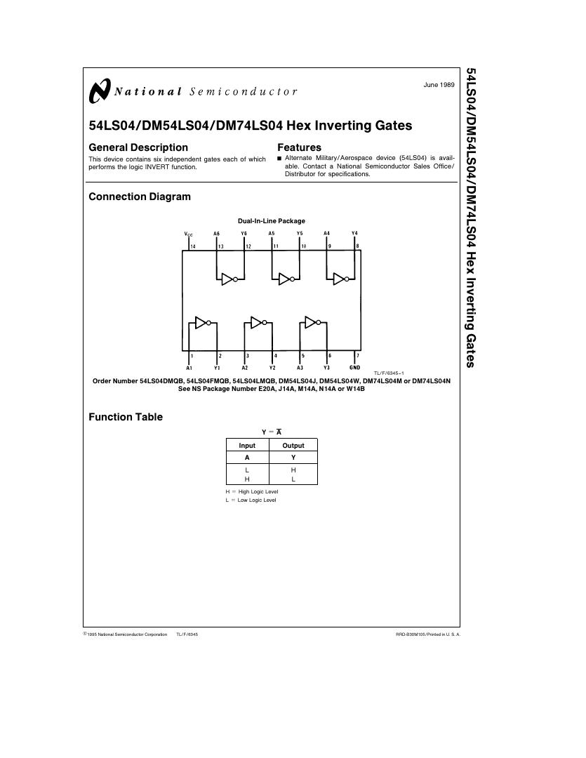
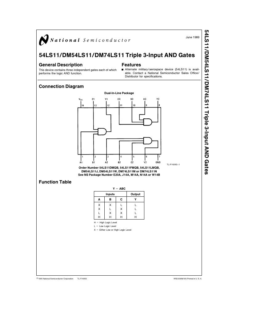
Integrated Circuits Used
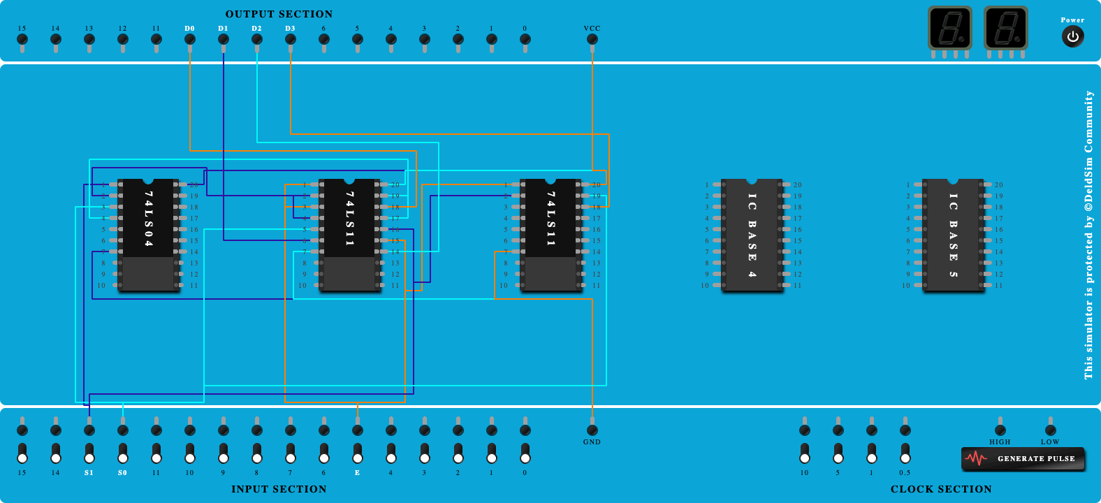
Circuit Tutorials
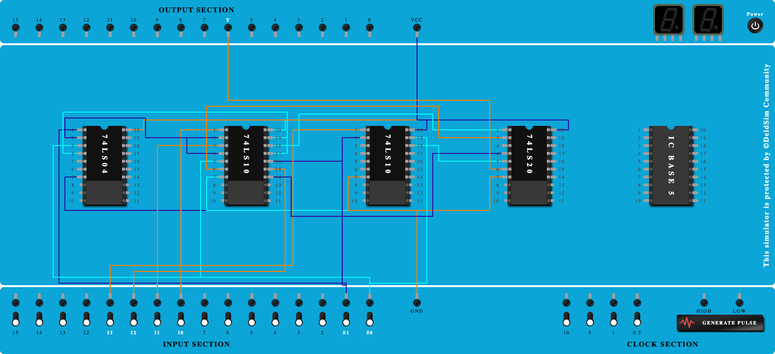
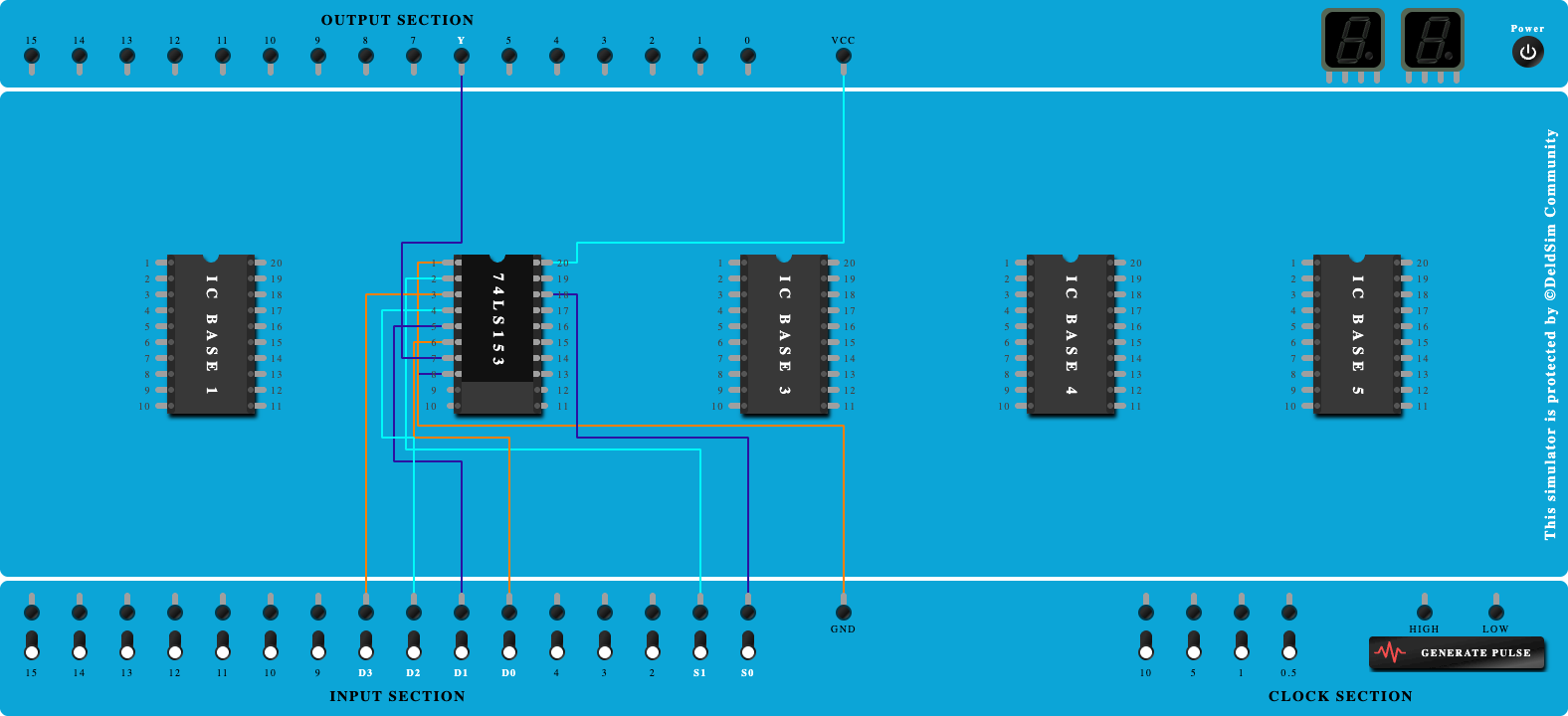
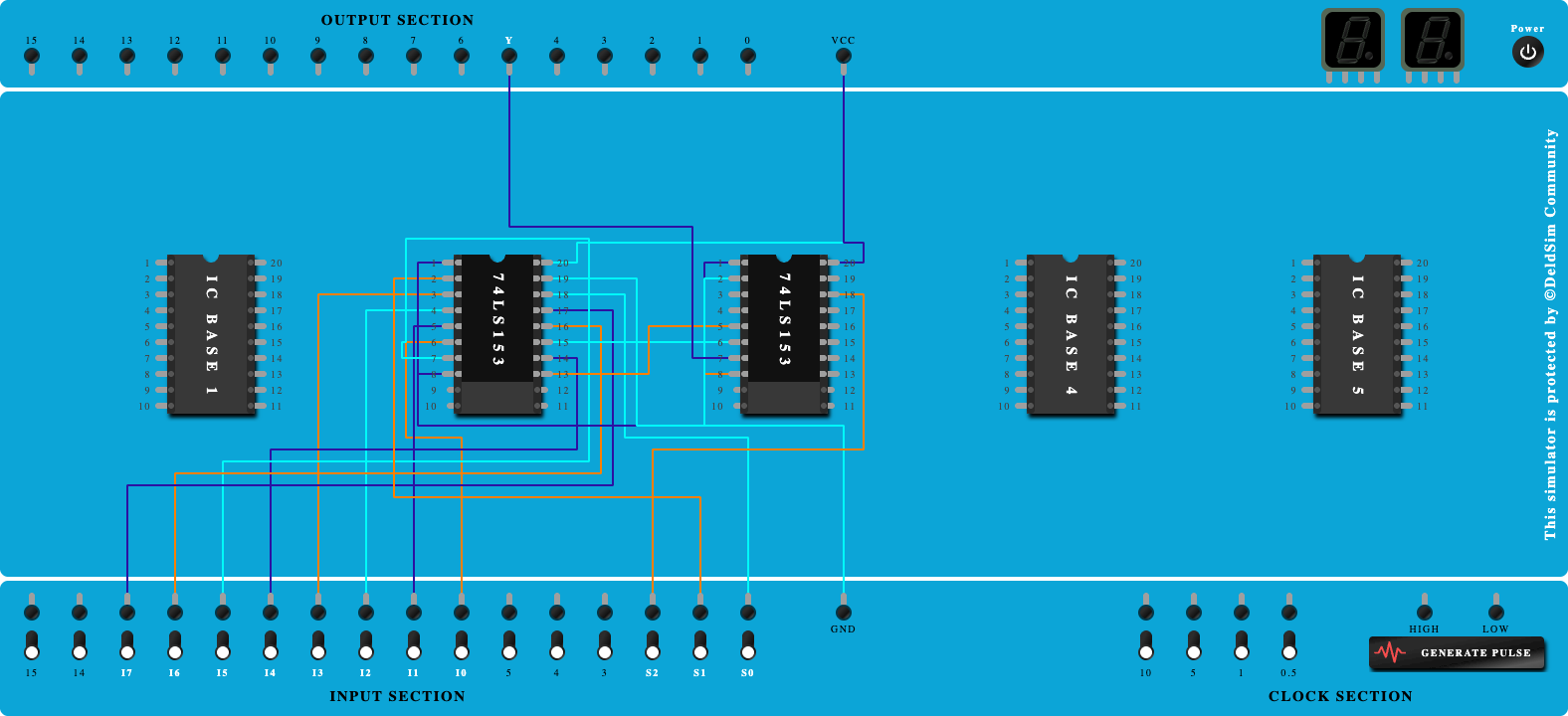
Procedure
- Place the IC on IC Trainer Kit.
- Connect VCC and ground to respective pins of IC Trainer Kit.
- Implement the circuit as shown in the circuit diagram.
- Connect the inputs to the input switches provided in the IC Trainer Kit.
- Connect the outputs to the switches of O/P LEDs
- Apply various combinations of inputs according to the truth table and observe the condition of LEDs.
- Note down the corresponding output readings for various combinations of inputs.
- Power Off Trainer Kit, disconnect all the wire connections and remove IC's from IC-Base.
Theory
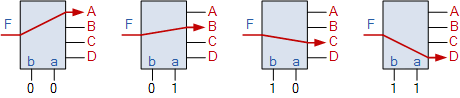
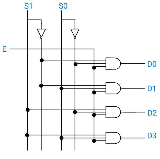
De-Multiplexer - The demultiplexer is a combinational logic circuit designed to switch one common input line to one of several separate output lines. The data distributor, known more commonly as a Demultiplexer or “Demux” for short, is the exact opposite of the Multiplexer we saw in the previous tutorial. The demultiplexer takes one single input data line and then switches it to any one of a number of individual output lines one at a time. The demultiplexer converts a serial data signal at the input to a parallel data at its output lines as shown below.
The function of the Demultiplexer is to switch one common data input line to any one of the 4 output data lines A to D in our example above. As with the multiplexer the individual solid state switches are selected by the binary input address code on the output select pins “a” and “b” as shown.
Demultiplexer Output Line Selection :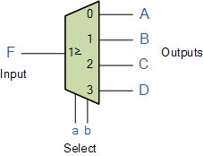
As with the previous multiplexer circuit, adding more address line inputs it is possible to switch more outputs giving a 1-to-2n data line outputs.
Some standard demultiplexer IC ́s also have an additional “enable output” pin which disables or prevents the input from being passed to the selected output. Also some have latches built into their outputs to maintain the output logic level after the address inputs have been changed.
However, in standard decoder type circuits the address input will determine which single data output will have the same value as the data input with all other data outputs having the value of logic “0”.
The Demultiplexer SymbolThe Demultiplexer Symbol
Block Diagram
Precautions
- Make the connections according to the IC pin diagram.
- The connections should be tight on trainer kit.
- The Vcc and ground should be applied carefully at the specified pin only.
Conclusion
Related Study Materials
Design and implement Multiplexer using gates

To study , design and implement Multiplexer using gates.
4:1 Multiplexer Using IC 74LS153
To study and Verify the 4:1 Multiplexer Using IC 74LS153.
8:1 Multiplexer using IC 74LS153
To study and Verify the 8:1 Multiplexer using IC 74LS153.