Learning Objectives
- To understand the behavior and demonstrate Full Adder function using 3:8 Decoder.
- To apply knowledge of the fundamental gates to create truth tables.
- To develop digital circuit building and troubleshooting skills.
- To understand key elements of TTL logic specification or datasheets.
Integrated Circuits Used


Circuit Tutorials
Procedure
- Place the IC on IC Trainer Kit.
- Connect VCC and ground to respective pins of IC Trainer Kit.
- Implement the circuit as shown in the circuit diagram.
- Connect the inputs to the input switches provided in the IC Trainer Kit.
- Connect the outputs to the switches of O/P LEDs
- Apply various combinations of inputs according to the truth table and observe the condition of LEDs.
- Note down the corresponding output readings for various combinations of inputs.
- Power Off Trainer Kit, disconnect all the wire connections and remove IC's from IC-Base.
Theory
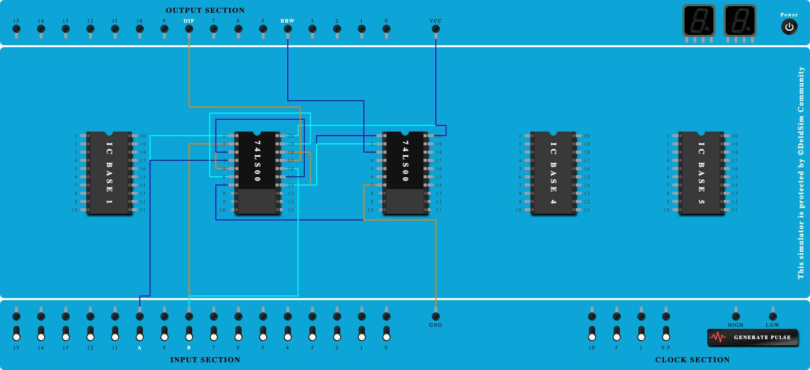
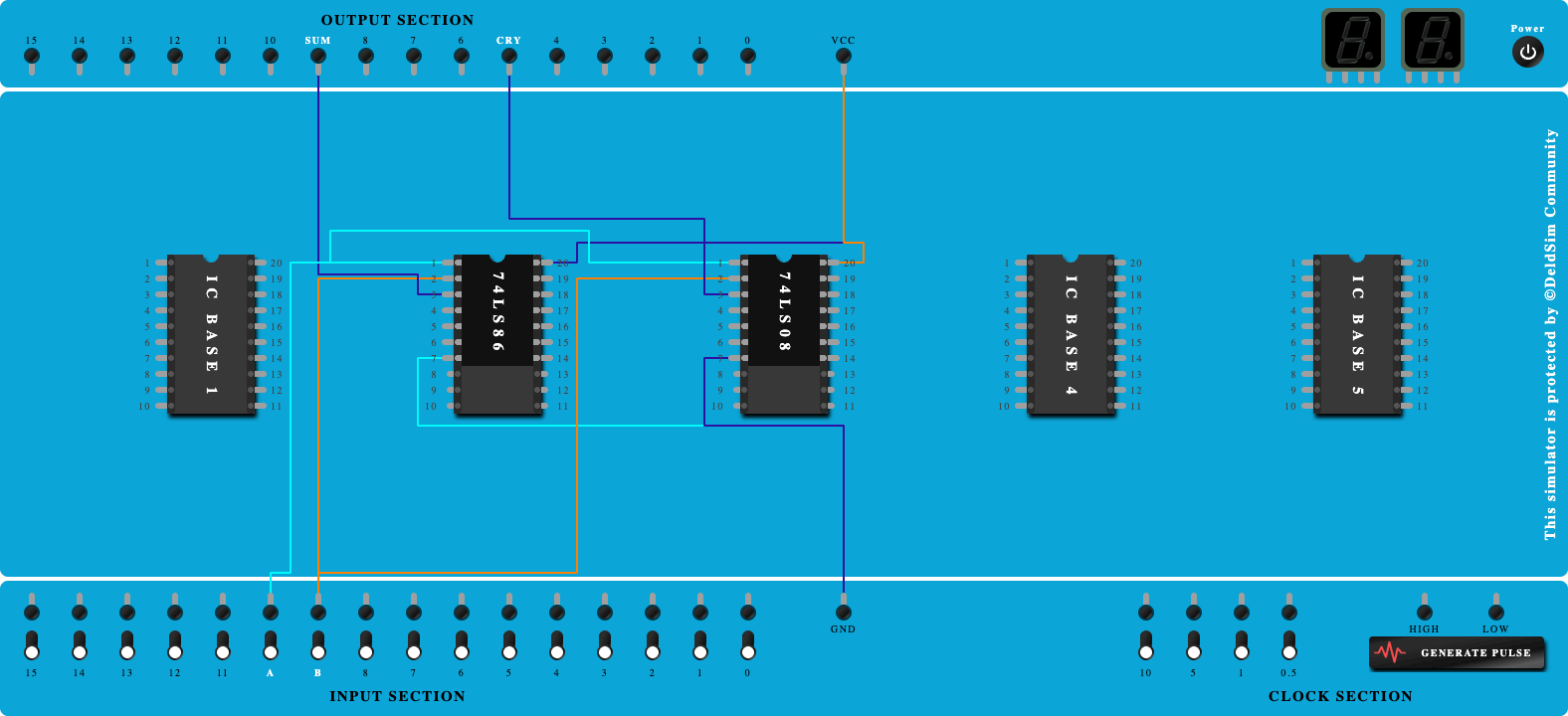
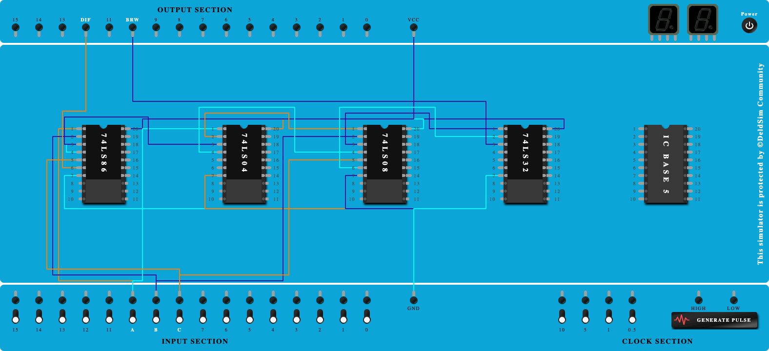
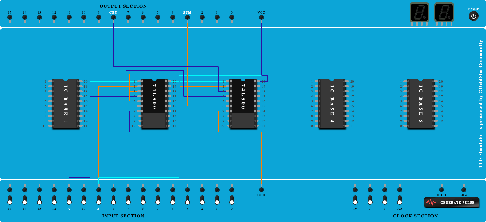
FULL ADDER - This adder is difficult to implement than a half-adder. The difference between a half-adder and a full-adder is that the full-adder has three inputs and two outputs, whereas half adder has only two inputs and two outputs. The first two inputs are A and B and the third input is an input carry as C-IN.
A full adder is a digital circuit that performs addition. Full adders are implemented with logic gates in hardware. A full adder adds three one-bit binary numbers, two operands and a carry bit. The adder outputs two numbers, a sum and a carry bit.
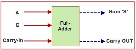
Then the full adder is a logical circuit that performs an addition operation on three binary digits and just like the half adder, it also generates a carry out to the next addition column. Then a Carry-in is a possible carry from a less significant digit, while a Carry-out represents a carry to a more significant digit.
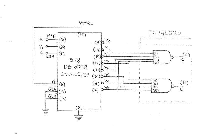
Decoder - A decoder is a combinational logic circuit which is used to change the code into a set of signals. It is the reverse process of an encoder. A decoder circuit takes multiple inputs and gives multiple outputs. A decoder circuit takes binary data of ‘n’ inputs into ‘2n’ unique output. In addition to input pins, the decoder has a enable pin. This enables the pin when negated, makes the circuit inactive.
3 Line to 8 Line Decoder - This decoder circuit gives 8 logic outputs for 3 inputs and has a enable pin. The circuit is designed with AND and NAND logic gates. It takes 3 binary inputs and activates one of the eight outputs. 3 to 8 line decoder circuit is also called as binary to an octal decoder.
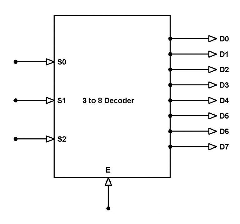
The decoder circuit works only when the Enable pin (E) is high. S0, S1 and S2 are three different inputs and D0, D1, D2, D3. D4. D5. D6. D7 are the eight outputs.
Block Diagram
Precautions
- Make the connections according to the IC pin diagram.
- The connections should be tight on trainer kit.
- The Vcc and ground should be applied carefully at the specified pin only.
Conclusion
Related Study Materials

Half subtractor using basic gates

To study and Verify the Half subtractor using basic gates.
Half Subtracter Using NAND Gates
To study and verify the Half Subtracter using NAND Gates.
Half Adder Using Basic Gates
To study and verify the Half Adder Using Basic Gates.
Full Subtractor using Two half adders basic gates
To study and Verify the Full Subtractor using Two half adders basic gates.
Half Adder using NAND Gates
To study and verify the Half Adder using NAND Gates.