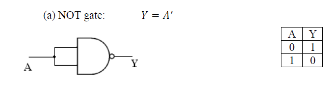
Implementation of NOT Gate using NAND gate
Aim
To study and verify the Implementation of NOT Gate using NAND gate.Learning Objectives
- To understand the behavior and demonstrate the Implementation of NOT Gate using NAND gate.
- To apply knowledge of the fundamental gates to create truth tables.
- To develop digital circuit building and troubleshooting skills.
- To understand key elements of TTL logic specification or datasheets.
IC Used
| IC Number | IC Name |
|---|---|
| 74LS00 | Quad 2-input NAND Gates |
Circuit Tutorials:
Procedure
- Place the IC on IC Trainer Kit.
- Connect VCC and ground to respective pins of IC Trainer Kit.
- Implement the circuit as shown in the circuit diagram.
- Connect the inputs to the input switches provided in the IC Trainer Kit.
- Connect the outputs to the switches of O/P LEDs
- Apply various combinations of inputs according to the truth table and observe the condition of LEDs.
- Note down the corresponding output readings for various combinations of inputs.
- Power Off Trainer Kit, disconnect all the wire connections and remove IC's from IC-Base.
Theory
NOT GATE - It is a digital circuit that has a single input and single output. The output of NOT gate is the logical inversion of input. Hence, the NOT gate is also called an inverter.
Logic NOT Gates are available using digital circuits to produce the desired logical function. The standard NOT gate is given a symbol whose shape is of a triangle pointing to the right with a circle at its end. This circle is known as an "inversion bubble". Logic NOT gates provide the complement of their input signal and are so called because when their input signal is "HIGH" their output state will NOT be "HIGH". Likewise, when their input signal is "LOW" their output state will NOT be "LOW". As they are single-input devices, logic NOT gates are not normally classed as "decision" making devices
Boolean Expression Y = A'
"If A is true, then Y is false"
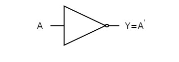
This NOT gate produces an output Y, which is the complement of input, A.
NAND gate - It is a digital circuit that has two or more inputs and produces an output, which is the inversion of logical AND of all those inputs.
Logic NAND Gates are available using digital circuits to produce the desired logical function and is given a symbol whose shape is that of a standard AND gate with a circle, sometimes called an "inversion bubble" at its output to represent the NOT gate symbol with the logical operation of the NAND gate.
As with the AND function seen previously, the NAND function can also have any number of individual inputs and commercial available NAND Gate IC's are available in standard 2,3, or 4 input types. If additional inputs are required, then the standard NAND gates can be cascaded together to provide more inputs.
Boolean Expression Y = (A.B)'
"If either A or B are NOT true, then Y is true"
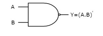
NAND gate operation is same as that of AND gate followed by an inverter. That's why the NAND gate symbol is represented like that.
Block Diagram
Precautions
- Make the connections according to the IC pin diagram.
- The connections should be tight on trainer kit.
- The Vcc and ground should be applied carefully at the specified pin only.
Conclusion
We have learned the Implementation of NOT Gate using NAND gate.Recommendations
2-Input AND Gate
Aim: To study and verify the truth table of 2-Input AND Gate.
ICs used: 74LS08 Implementation of NAND Gate using NOR gate
Aim: To study and verify the Implementation of NAND Gate using NOR gate.
ICs used: 74LS02 Implementation of Ex-OR Gate using NAND gate
Aim: To study and verify the Implementation of Ex-OR Gate using NAND gate.
ICs used: 74LS00 Implementation of Ex-NOR Gate using NAND gate
Aim: To study and verify the Implementation of Ex-NOR Gate using NAND gate.
ICs used: 74LS00 Implementation of NOR Gate using NAND gate
Aim: To study and verify the Implementation of NOR Gate using NAND gate.
ICs used: 74LS00